

Semiconductor Sector India: Complete Analysis 2026
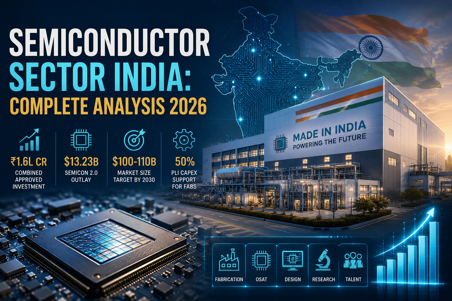
Semiconductor sector in India has moved from a policy ambition to physical, operational infrastructure faster than almost any other industrial theme in the country's recent history. Micron's assembly and test facility in Sanand, Gujarat was inaugurated by the Prime Minister on February 28, 2026 — the first operational facility of the current mission cycle — and by mid-2026, six approved projects worth a combined ₹1.6 lakh crore were either operational or under advanced construction.
We wanted to separate what's genuinely built and running today from what remains ambition, since semiconductor coverage in Indian media often blurs the two together. This is a sector where the difference between "approved" and "operational" matters enormously for anyone trying to actually assess investment merit.
Table of Contents
- From Policy Document to Construction Site
- The Six Approved Facilities
- Semicon 2.0: The Bigger Second Wave
- How the PLI Incentives Actually Work
- The Real Market Size Opportunity
- Real Example: Understanding What "28nm" Means for India
- Key Listed Players to Understand
- Key Risks Worth Understanding
- How to Approach This Sector
- Frequently Asked Questions
From Policy Document to Construction Site
The India Semiconductor Mission was approved by the Union Cabinet in December 2021 with an initial ₹76,000 crore outlay, operationalized under the Ministry of Electronics and Information Technology. For years, this remained largely a policy framework with limited physical output. That changed decisively through 2025 and 2026: Micron's Sanand ATMP (Assembly, Test, Marking, and Packaging) facility became fully operational, Kaynes Semicon's OSAT facility in Sanand was inaugurated March 31, 2026, and Tata Electronics' semiconductor assembly and test facility in Jagiroad, Assam is now running.
The Six Approved Facilities
India's Approved Semiconductor Projects (Mid-2026)
| Facility | Partner | Location | Status |
|---|---|---|---|
| Micron ATMP | Micron Technology ($2.75B) | Sanand, Gujarat | Operational (Feb 2026) |
| Tata-PSMC Fab | Tata Electronics + Powerchip (Taiwan), ASML | Dholera, Gujarat | Under construction, first silicon targeted late 2026 |
| Tata Semiconductor Assembly & Test | Tata Electronics | Jagiroad, Assam | Operational |
| CG Power-Renesas-Stars OSAT | CG Power | Sanand, Gujarat | Pilot line inaugurated Aug 2025 |
| Kaynes Semicon OSAT | Kaynes Technology | Sanand, Gujarat | Operational (March 2026) |
| HCL-Foxconn Display Driver IC Fab | HCL + Foxconn JV | Jewar, Uttar Pradesh | Groundbreaking stage |
The Tata-PSMC Dholera fab is genuinely the centerpiece of this mission — it's India's first front-end wafer fabrication facility, backed by an estimated $11 billion investment, targeting 28nm and below process nodes. This isn't the 2nm frontier chip territory that Taiwan's TSMC or Korea's Samsung operate in, but it covers the mature-to-advanced range relevant to automotive chips, industrial microcontrollers, display drivers, and IoT devices — genuinely useful, commercially significant chip categories even without bleeding-edge node capability.
Semicon 2.0: The Bigger Second Wave
On July 15, 2026, the government announced Semicon 2.0, allocating ₹1.275 trillion (roughly $13.23 billion) — a dramatically larger commitment than the original ₹76,000 crore mission outlay. This second wave broadens support across the entire ecosystem: chip design, fabrication, display manufacturing, advanced packaging, semiconductor equipment, specialty materials, R&D, and talent development, rather than concentrating support narrowly on fab construction alone.
Semicon 2.0 vs Original Mission
| Program | Outlay | Focus |
|---|---|---|
| India Semiconductor Mission (2021) | ₹76,000 crore | Fabs, ATMP, compound semiconductors |
| Electronics Component Manufacturing Scheme (2025) | ₹22,919 crore | Upstream components: PCBs, packaging materials, specialty chemicals |
| Semicon 2.0 (July 2026) | ₹1.275 trillion (~$13.23B) | Full ecosystem: design, fabrication, equipment, talent |
The Electronics Component Manufacturing Scheme specifically targets the upstream supply chain — PCB substrates, advanced packaging materials, test socket components, and specialty chemicals — the less glamorous but genuinely essential inputs that any domestic semiconductor ecosystem needs beyond just the headline fab announcements. Several tier-1 component manufacturers from Japan, South Korea, and Taiwan have already filed expressions of interest to establish India manufacturing under this scheme.
How the PLI Incentives Actually Work
The Production Linked Incentive structure offers meaningfully different support levels depending on the type of facility: up to 50% of capital expenditure for new fabs, up to 25% for ATMP/OSAT (assembly, testing, marking, and packaging) units, and 50% fiscal support specifically for Scheme C, covering compound semiconductors and MEMS (specialty manufacturing).
Why This Incentive Structure Matters for Investment Decisions
The disbursement data is genuinely worth noting: the India Semiconductor Mission had disbursed approximately ₹18,000 crore as of early 2026, with the remainder committed as facilities hit specific production milestones — meaning this fiscal commitment is real and actively flowing, not merely aspirational budget-line promises. For investors evaluating semiconductor-linked companies, checking whether a company's project has actually cleared milestone-linked disbursement gates (versus simply being "approved" on paper) is a genuinely useful due-diligence signal that separates real progress from press-release momentum.
The Real Market Size Opportunity
India's semiconductor market was roughly $38 billion in 2023, grew to $45-50 billion by 2024-25, and is projected to reach $100-110 billion by 2030 — driven by rising integration of chips across aerospace, automobiles, communications, IT, clean energy, and defense sectors, alongside surging domestic demand for smartphones and data storage. India's stated strategic goal is capturing 1-2% of the global semiconductor market by 2030, which sounds modest in percentage terms but represents a genuinely substantial absolute opportunity given the sheer scale of the global semiconductor industry.
India Semiconductor Market Trajectory
| Year | Market Size |
|---|---|
| 2023 | ~$38 billion |
| 2024-25 | $45-50 billion |
| 2030 (Projected) | $100-110 billion |
Real Example: Understanding What "28nm" Means for India
Why the Dholera Fab's Node Target Actually Matters
The Tata-PSMC Dholera fab targeting 28nm and below process nodes is a genuinely deliberate strategic choice, not a limitation to apologize for. While TSMC and Samsung compete at 2-3nm for flagship smartphone processors and AI chips, the 28nm range covers an enormous, stable market: automotive control units, industrial sensors, power management chips, and display drivers — categories where demand is arguably more predictable and less cyclically volatile than cutting-edge AI chip demand. India entering at this node range plays directly to genuine near-term strengths (established process technology, lower capital intensity per fab than leading-edge nodes) rather than attempting to leapfrog directly into a race against far more mature competitors.
Key Listed Players to Understand
The listed universe touching India's semiconductor buildout spans several genuinely distinct categories: Tata Electronics (part of the broader Tata Group, though not independently listed at the fab-project level), CG Power (listed, directly involved in OSAT), Kaynes Technology (listed, OSAT operator), and a broader ecosystem of component and equipment suppliers benefiting indirectly from the buildout. This mirrors the same sub-segment differentiation we've highlighted in our defense sector analysis and renewable energy sector analysis — treating "semiconductor stocks" as one undifferentiated basket misses genuinely important distinctions between pure-play fab operators, OSAT/ATMP specialists, and indirect beneficiaries in the broader supply chain.
Key Risks Worth Understanding
What Could Slow This Down
1. India isn't yet in advanced-node territory. Taiwan and South Korea continue to dominate cutting-edge chip production; India's near-term strategy deliberately targets mature nodes, which limits addressable market to specific chip categories rather than the full semiconductor spectrum.
2. High capital costs and skilled labor shortages. Semiconductor manufacturing remains genuinely capital-intensive and requires specialized technical talent that India is still actively building out.
3. Intense global competition for the same incentive-seeking capital. The US, EU, Japan, and other nations are simultaneously offering substantial subsidies to attract semiconductor investment, meaning India competes globally for the same pool of manufacturers and capital.
4. Execution timeline risk. First silicon at Dholera is targeted for late 2026 — a milestone worth tracking closely, since delays in flagship projects can meaningfully affect broader sector sentiment even if the underlying policy support remains intact.
How to Approach This Sector
Given how early-stage much of this sector genuinely remains — several flagship facilities are still under construction or newly operational — a patient, staggered approach makes sense here as it does for other structurally-promising but execution-dependent themes we've covered, similar to our framing in the renewable energy green hydrogen discussion. Investors specifically want to distinguish between direct semiconductor plays and the broader electronics manufacturing ecosystem that benefits indirectly from this buildout, since the latter category is considerably larger and includes many companies with more established earnings track records than the newer, more speculative pure-play semiconductor names.
Readers tracking related technology and manufacturing themes may also find our IT sector AI-led recovery analysis a useful companion read, since semiconductor availability and AI infrastructure buildout are genuinely interconnected trends, and our sector rotation piece for understanding how emerging, high-growth themes like semiconductors typically behave across different phases of broader market sentiment.
It's also worth situating this sector within the broader global supply-chain diversification narrative. As countries increasingly seek alternatives to concentrated chip manufacturing in Taiwan and China, India's positioning benefits from geopolitical tailwinds that are genuinely distinct from the domestic policy support covered above — this connects to themes we've explored in our India-US trade deal coverage and H1B visa fee impact on Indian IT piece, since technology talent mobility and manufacturing supply-chain shifts are often discussed as part of the same broader US-India economic relationship.
Investors weighing semiconductor exposure alongside other high-conviction manufacturing themes may also find our defense sector analysis a useful parallel read, since both sectors share a common structural pattern: substantial government policy support, multi-year execution timelines, and a genuine gap between headline announcement value and actually operational, revenue-generating capacity that disciplined investors need to track carefully rather than assume away.
Frequently Asked Questions
What is India's semiconductor market size expected to reach by 2030?
India's semiconductor market is projected to grow from $45-50 billion (2024-25) to $100-110 billion by 2030, as India aims to capture 1-2% of the global semiconductor market.
What is the Tata-PSMC Dholera fab and when will it be operational?
It's India's first front-end wafer fabrication facility, an $11 billion investment targeting 28nm and below process nodes, with first silicon targeted for late 2026.
Is India competing with Taiwan and South Korea in advanced chip manufacturing?
Not directly yet. India's current facilities target mature nodes (28nm and below) covering automotive, industrial, and IoT chip categories, rather than the 2-3nm cutting-edge nodes where TSMC and Samsung dominate.
How much has India actually invested in semiconductor manufacturing so far?
The India Semiconductor Mission had disbursed approximately ₹18,000 crore as of early 2026, with six approved projects worth a combined ₹1.6 lakh crore either operational or under construction.
What is Semicon 2.0?
Semicon 2.0, announced July 15, 2026, is a ₹1.275 trillion (~$13.23 billion) expanded government initiative covering chip design, fabrication, display manufacturing, advanced packaging, equipment, and talent development across the full semiconductor ecosystem.
What are the main risks to India's semiconductor ambitions?
India isn't yet in advanced-node territory, faces high capital costs and skilled labor shortages, competes globally against other nations offering similar incentives, and carries execution timeline risk on flagship projects like the Dholera fab.

Pranab Barman is a Financial Educator and Personal Finance Researcher with over 10 years of hands-on experience in stock markets, trading, and investing. Currently enrolled in the CFA Program, he is committed to continuous learning and professional excellence in finance.
As the Founder of PlayWithStock, Pranab covers a wide range of topics including Mutual Funds, SIP, Taxation, Stock Market Basics, and Financial Calculators — with a focus on simplifying complex financial concepts for everyday all investors.
Email: support@playwithstock.com
Website: playwithstock.com
Related posts:
 Stocks to Buy After India-US Trade Deal 2026: A Sector-by-Sector Breakdown
 PSU Bank Stocks Sector Analysis: Why They Outperformed in 2025-26
 AI Investing 2026: The Complete India-US Stock Guide
 Jio Financial Services Q1 FY27 Results Preview: Date, Estimates & Stock Analysis
 What Is Sector Rotation? A Simple Guide for Indian Investors
 What is Nifty Midcap 150? Complete Guide and Should You Invest in 2026
 Nifty July 2026: Will It Hit 24,800? Complete Market Outlook and Stock Guide
 50-50 Cash Margin Rule: The Complete Guide to Structuring Capital Efficiency in 2026